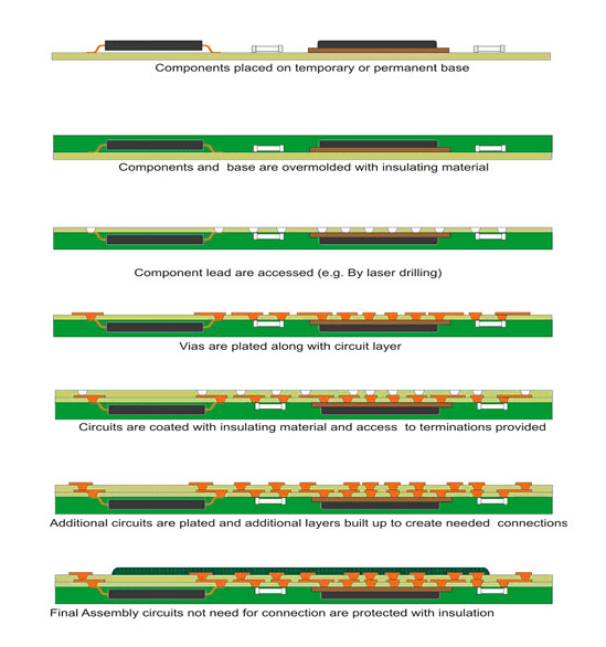
The basic idea is to build electronic assemblies in reverse. That is the manufacturer first bonds in place tested and burned in IC packages and various discrete components directly on to a carrier in predetermined locations and then encapsulates the components so that they become a monolithic assembly. A cleaning/abrading step will provide direct access to the contact of the components, which it is anticipated will be copper. Alternatively, a laser can be used to ablate any material covering the leads. The assembly can be then metallized with copper and circuit patterns created to make the required interconnections between leads of all of the various components. If more than one layer is required, the process can be repeated multiple times until all required interconnections are made. The final circuit layer can then be coated with an insulator connected to whatever user interfaces, displays and power connections are required for operation.
Download the White (Green) Paper